

Discrete Electronic Components, General ICs, ICs
CD4011 CMOS Quad 2-Input NAND Gate IC
₨36.00
Propagation delay time = 60 ns (typ.) at CL = 50 pF, VDD= 10 V
Buffered inputs and outputs
Standardized symmetrical output characteristics
Maximum input current of 1 µA at 18 V over-full package temperature range; 100 nA at 18 V and 25°C
100% tested for quiescent current at 20 V
5-V, 10-V, and 15-V parametric ratings
Noise margin (over full package temperature range:
1 V at VDD = 5 V
2 V at VDD = 10 V
2.5 at VDD = 15 V
Meets all requirements of JEDEC Tentative Standard No. 13B, “Standard Specifications for Description of “B” Series CMOS Devices”
Related products
-
Discrete Electronic Components
1K Ohm 102 Horizontal Type Trimpot Potentiometer / Variable Resistor
₨18.00 Add to cart -
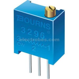
Discrete Electronic Components
10K Ohm 103 Multi turn Trimpot Potentiometer / Variable Resistor
₨36.00 Add to cart


Reviews
There are no reviews yet.